

There’s been no greater act of magic in technology than the sleight of hand performed by Moore’s Law. Electronic components that once fit in the palm of your hand have long gone atomic, vanishing from our world to take up residence in the quantum realm.
But we’re now brushing the bitter limits of this trend. In a paper published in Nature this week, scientists at Tsinghua University in Shanghai wrote that they’ve built a graphene transistor gate with a length of 0.34 nanometers (nm)—or roughly the size of a single carbon atom.
The gate, a chip component that switches transistors on and off, is a critical measure of transistor size. Previous research had already pushed gate lengths to one nanometer and below. By scaling gate lengths down to the size of single atoms, the latest work sets a new mark that’ll be hard to beat. “In the future, it will be almost impossible for people to make a gate length smaller than 0.34 nm,” the paper’s senior author Tian-Ling Ren told IEEE Spectrum. “This could be the last node for Moore’s Law.”
Etching a 2D Sandwich
Transistors have a few core components: the source, the drain, the channel, and the gate. Electrical current flows from the source, through the channel, past the gate, and into the drain. The gate switches this current on or off depending on the voltage applied to it.
Recent advances in extreme transistor gate miniaturization rely on some fascinating materials. In 2016, for example, researchers used carbon nanotubes—which are single-atom-thick sheets of carbon rolled into cylinders—and a 2D material called molybdenum disulfide to achieve a gate length of one nanometer. Silicon is a better semiconductor, as electrical currents encounter more resistance in molybdenum disulfide, but when gate lengths dip below five nanometers, electrons leak across the gates in silicon transistors. Molybdenum disulfide’s natural resistance prevents this leakage at the tiniest scales.
So, building on the prior work, the researchers in the recent study also chose to use molybdenum disulfide for their channel material and a carbon-based gate.
But instead of carbon nanotubes, which are a nanometer across, they looked to go smaller. Unroll a carbon nanotube and you get a sheet made of carbon atoms called graphene. Graphene has all kinds of interesting properties, one of which is excellent conductivity. The width and length of a graphene sheet are, of course, bigger than a nanotube—but the edge is a single carbon atom thick. The team cleverly exploited this property in their work.
First they laid down a layer of silicon for the base structure. Then, using a graphene production method called chemical vapor deposition, they laid a sheet of graphene on top of the silicon dioxide and a layer of aluminum oxide on top of the graphene. The aluminum oxide and silicon dioxide sandwiching the graphene act as insulators, effectively cutting off its electrical properties from the rest of the transistor. They then etched into the sandwiched materials to create a step—the same shape as the stairs in your home—and to expose just the edge of the graphene sheet in the vertical wall of the step, thus making an atomically thin gate. They call this clever construction a “sidewall transistor.”
Over the step, the team laid down a layer of hafnium oxide—to add a little space between gate and channel—and a layer of molybdenum disulfide to form the channel. They then added electrodes, one on the top step and one on the bottom, as source and drain.
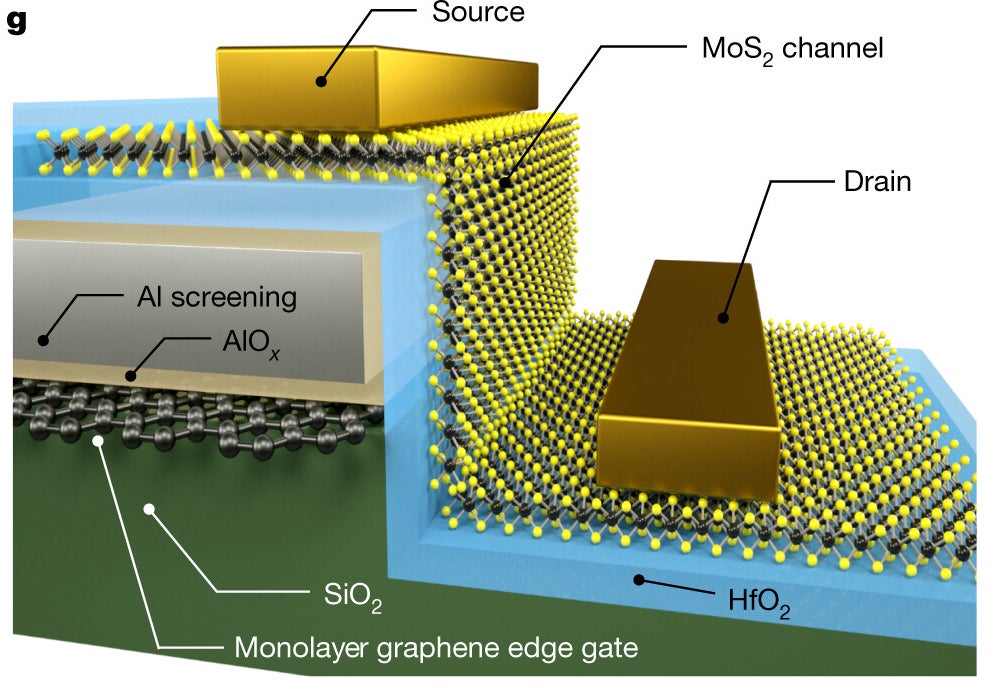
Critically, the new technique doesn’t require the researchers to precisely position the graphene to make the gate work. This is one of the big challenges of using carbon nanotubes—it’s no mean feat getting them to settle in exactly where they’re needed.
More Moore
To be clear, the work is a proof of concept: The researchers haven’t meaningfully scaled the approach. Fabricating a handful of transistors isn’t the same as manufacturing billions on a chip and flawlessly making billions of those chips for use in laptops and smartphones. Ren also points out that 2D materials, like molybdenum disulfide, are still pricey and manufacturing high-quality stuff at scale is a challenge.
New technologies like gate-all-around silicon transistors are more likely to make their way into your laptop or phone in the next few years. Also, it’s worth noting that the upshot of Moore’s Law—that computers will continue to get more powerful and cheaper at an exponential pace—can also be driven by software improvements or architecture changes, like exploiting the third dimension and stacking components on top of one another.
Still, the research does explore and better define the bitter edge of miniaturization, perhaps setting a lower bound that may not be broken for years. It also demonstrates a clever way to exploit the most desirable properties of 2D materials in chips. And if further refined, the approach, which doesn’t rely on the exact positioning of components and leans on already common chipmaking technologies, does seem to have some potential to scale.
Regardless, shrinking the size of electronic components from inches to atoms over a relatively short span of decades remains one of science and technology’s niftiest tricks.
Image Credit: Yulissa Tagle / Unsplash
* This article was originally published at Singularity Hub


0 Comments